Noise Generator
The noise waveform is generated taking the output of eight selected bits from a 23 bit Fibonacci LFSR. There are actually 24 bits on chip but the last one is unused. The register is clocked when bit 19 of the oscillator goes high and has taps at bits 17 and 22.
Each bit is formed by two inverters feeding each other through the gates c1 and c2, while the gate LC controls the shifting. The output from bits 0, 2, 5, 9, 11, 14, 18 and 20 is sent to the waveform selector.


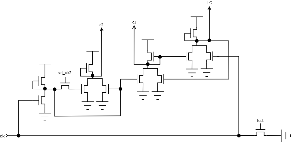
The bit gates c1, c2 and LC are controlled by the following clock generator. When the test bit is set clk is grounded, so the c1 and c2 gates are open and the LC gate is closed, connecting adjacent bits. This means that setting and resetting the test bit forces a shift of the register pushing an 1 in the feedback XOR. Also the register can be "reset" using the test bit: the c1 gate stays open and the output inverters slowly settle high at a speed dependent on the manufacturing spec of the chip.

The outputs results from the following expressions:
- c2 = ¬(¬clk_phi2 ∨ ¬clk) = clk_phi2 ∧ clk
- c1 = ¬(¬clk ∨ LC) = clk ∧ ¬LC
- LC = ¬(c1 ∨ clk) = ¬clk ∧ ¬c1
 clk | c1 c2 LC
-----|----------
  1  | 1  1  0
  0  | 0  0  1
  1  | 1  0  0
  1  | 1  1  0
The clk signal in the above picture is derived from the output of oscillator's bit 19:


The output results from the following expression:
- clk = ¬(sid_rst ∨ test ∨ (bit19[t-1] ∧ ¬bit19[t-2]))
t | bit19 | clk
--|-------|-----
0 |   0   |  1
1 |   1   |  1   <- bit19 raises
2 |   1   |  0   <- shift phase 1
3 |   1   |  1   <- shift phase 2
t | test  | clk
--|-------|-----
0 |   0   |  1
1 |   1   |  0   <- test set - shift phase 1
. |   1   |  0
n |   0   |  1   <- test released - shift phase 2
When shifting bit 0 is fed with the XOR of bits 17 and 22, unless the test bit is set, in which case the bit 17 is inverted (XORed with 1).

The output results from the following expression:
- bit0 = ¬((ns17 ∧ a) ∨ b) = ¬(ns17 ∧ a) ∧ ¬b
where:
- a = (/reset_phi2 ∨ test_phi2 ∨ ns22)
- b = ¬(ns17 ∨ a)
resulting in:
- bit0 = ¬(ns17 ∧ a) ∧ (ns17 ∨ a) = ns17 ⊕ A = ns17 ⊕ (/reset_phi2 ∨ test_phi2 ∨ ns22)

According to the timing diagrams and the schematics the shift is performed in two steps and starts one cycle after bit 19 of the oscillator goes high. The following table shows the noise clock status during shifting:
     | bit19 | clk | LC c1 c2 |
-----|-------|-----|----------|
phi1 |   0   |  1  | 0  1  1  |
phi2 |   0   |  1  | 0  1  1  |
-----|-------|-----|----------|
phi1 |   1   |  1  | 0  1  1  | <- bit19 raises
phi2 |   1   |  1  | 0  1  1  |
-----|-------|-----|----------|
phi1 |   1   |  0  | 1  0  0  | <- shift phase 1
phi2 |   1   |  0  | 1  0  0  |
-----|-------|-----|----------|
phi1 |   1   |  1  | 0  1  0  | <- shift phase 2
phi2 |   1   |  1  | 0  1  1  |
In the first step bits are interconnected and the output of each bit is latched into the following. In the first clock half of the second step the latched value becomes active.
    bit n     |   bit n+1
 latch output | latch output
--------------|--------------
   A <-> A    |   B <-> B
   A <-> A    |   B <-> B
--------------|--------------
   A <-> A    |   B <-> B
   A <-> A    |   B <-> B
--------------|--------------
   X     A  --|-> A     B      <- shift phase 1
   X     A  --|-> A     B
--------------|--------------
   X --> X    |   A --> A      <- shift phase 2
   X <-> X    |   A <-> A
If test or reset signals are active the phase 1 is repeated at each cycle until the signal is released triggering the second phase.