Address Decoders
The first bits for the address decoding are the CS and R/W pins. CS is the active low chip select signal while R/W controls the data flow direction. More details on the pins and the timings can be found in the reference

Both the read and write operations are controlled through NOR gates using the CS, Phi2 and RW signals as input.
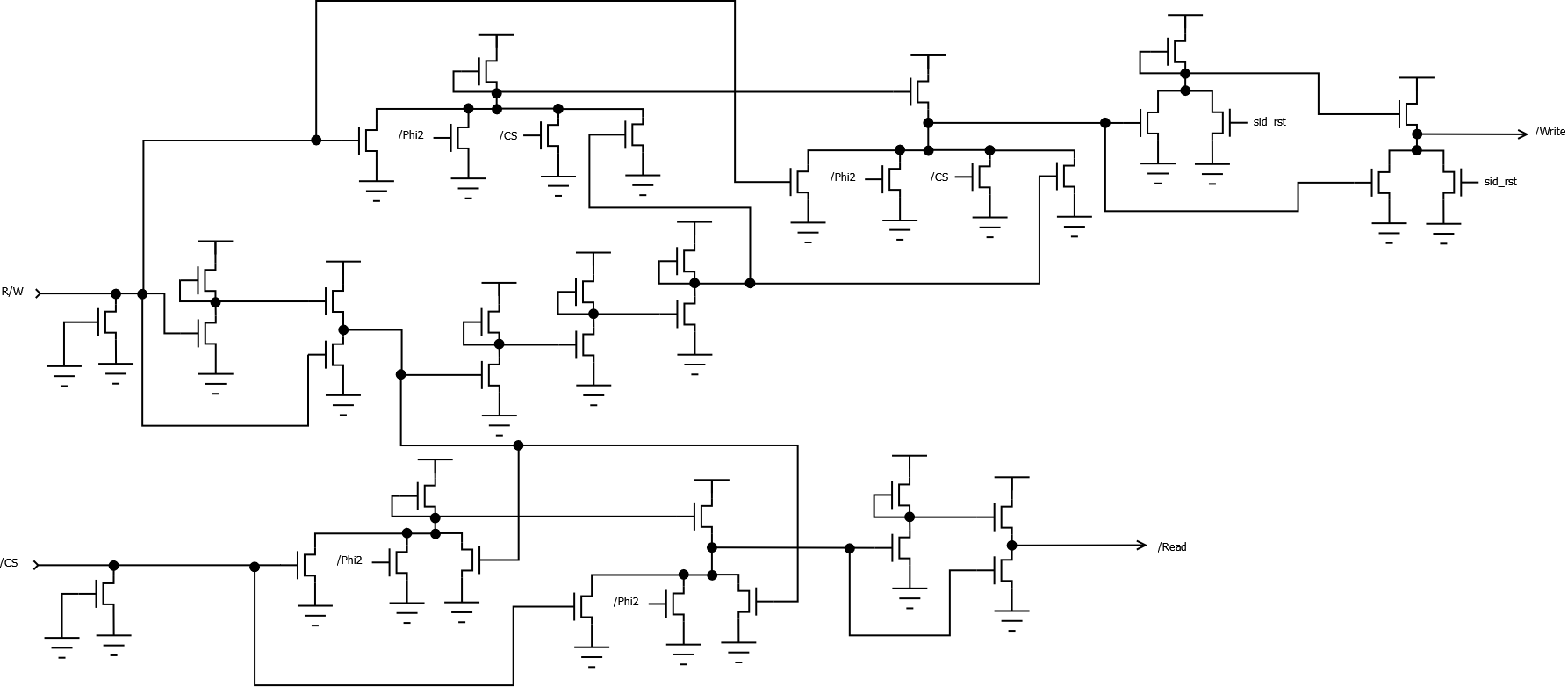
The resulting expressions are:
- /Write = ¬(¬(RW ∨ ¬Phi2 ∨ /CS ∨ _RW) ∨ sid_rst) = (RW ∨ ¬Phi2 ∨ /CS ∨ _RW) ∧ ¬sid_rst
- /Read = ¬(¬(/CS ∨ ¬Phi2 ∨ ¬RW)) = /CS ∨ ¬Phi2 ∨ ¬RW
where _RW is the RW signal slightly delayed by passing through a few inverters, likely to give the data bus some time before doing the actual writing.
The read/write operations are then done when CS is low and Phi2 is high. When RW is high a read is performed otherwise it's a write. During reset the /Write line is low while /Read is high, meaning that every register is written to as we will see that all the address lines are low too.
Then there are five address pins, from A0 to A4, to allow indexing the 29 chip registers.

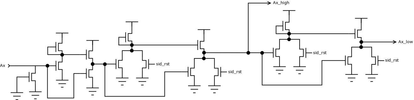
Some big transistors to control timings, but basically this produces two signals, one of which is high when the line is high and the other when it's low. During reset both signals are held at zero.
These are two address decoders for the read-only register $1B (OSC3) on the left and the write-only register $12 (CR3) on the right.

Each decoder just NORs the five address lines and the read/write line, taking as input either the active low or the active high ones depending on the register's address and function. A register is therefore activated when all of its inputs are low.
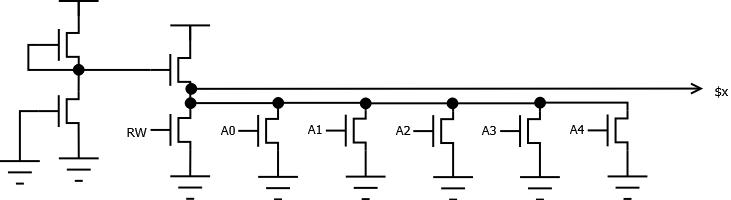
For example the line $1B is active only when the address bus has the value 11011, so if one or more of the A4_low, A3_low, A2_high, A1_low or or A0_low lines are high the decoder outputs a zero. This also happens, being a read-only register, when the write line is high.
This is the full map of the address decoders:
